- Home
- Home_de
- Products
- Downloads
- Forum
- Sales
- News
- Exhibitions
- Know how
- Building VP-2500D workingtable
- First installation
- VP-2500D 0402 placement test
- Mark detection demo
- Placing TQFP48 demo
- 0201 Placement
- BGA Alignment
- FAQ-Feeder-settings
- Soldering-FAQ
- Controller Upgrade V1 to V2
- How to upgrade to 19 slot nozzle changer
- First setup and placement job
- How to build Electronics
- For Makers
- Questions & Answers
- Software
- Repair Documents
- References
- Service
- Spare-Parts
- Videos
- Warranty
- Kompetenz
- Competence
- Cookie Policy
- Privacy Policy
- About
- PANDA-design-contest

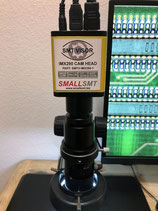
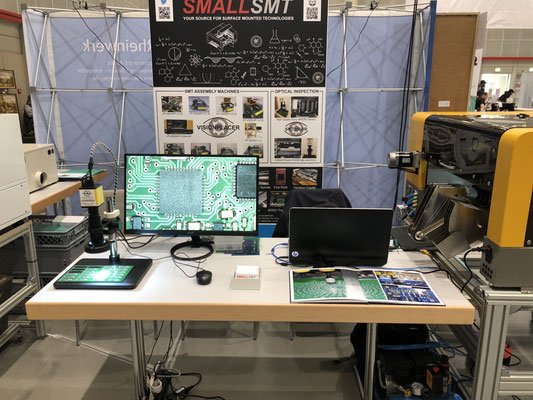
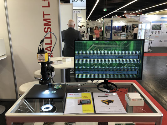
We offer our new SMT VISOR System for optical PCB inspection
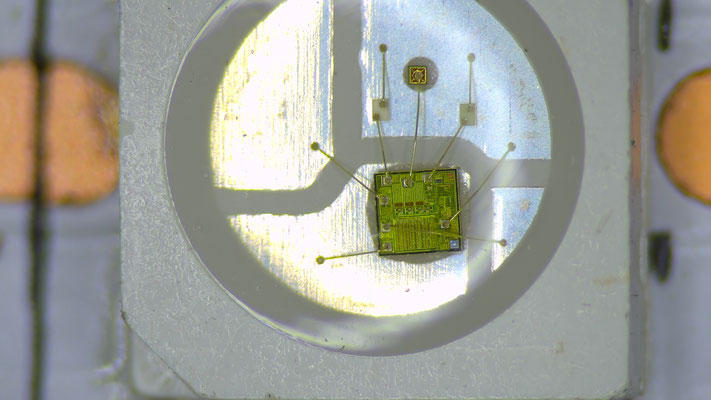
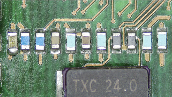
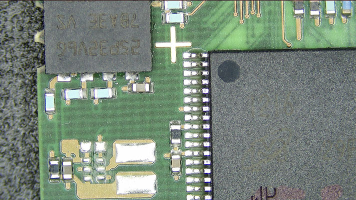
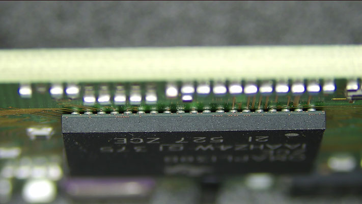
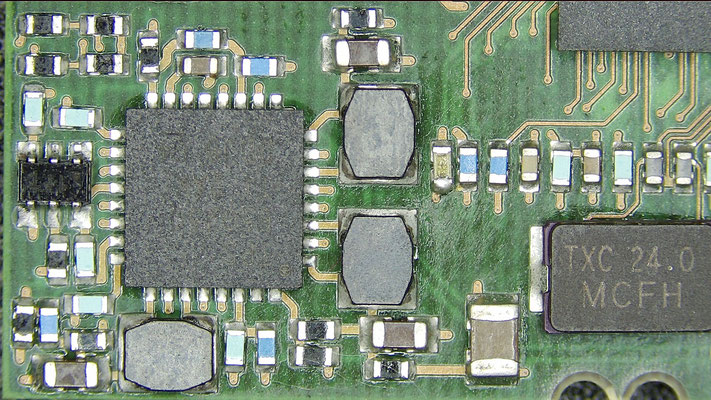
This microscope system offer brilliant image quality without latency on HDMI output.
It has fast zoom and offer wide range automatic image adjustment.
The depth of field is perfect thanks to the built-in HDR function.
PCB repair jobs and SMT inspection has never been easier.
Take a look for the WS2812 LED photo in the gallery!
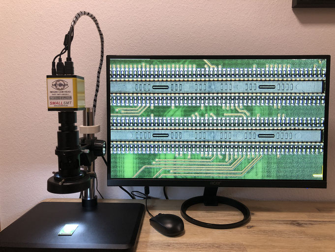
CAMERA UI
GALLERY
TECHNICAL DATA
Lens: 16X-160X Adjustable Magnification 25mm Zoom C-mount Lens 0.7X~5X, working distance 105mm
Camera: IMX290 Sony 2,2MP Camera chip, wide range automatic zoom, HDR,
BSI high light sensitive sensor
Pixel size : 1/2.8"
Lens interface : C / CS type
Exposure : automatic and manual
Display frame rate : 60Hz at 1080P
Shutter Speed : 1/50s(1/60s)~1/10000s

You can buy a HDMI to USB Video grabber to digitize the camera output. This cheap device found on AMAZON.
https://www.amazon.de/dp/B07FTLBRSG/ref=psdc_1626220031_t2_B07BGXVGLS
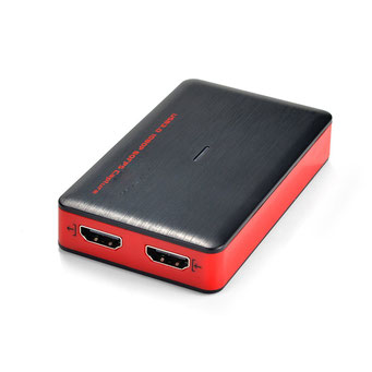
This one has HDMI pass through so Monitor can keep connected during capture.

SMTV-IMX290-1 PCB Inspection System
Camera Head IMX290, Microscope zoom lens, Stand, Mouse, HDMI cable, standard LED ring light, Power supply
$1,100.00
Final price excl. shipping costs
Free shipping to the following countries: Show more Show less
- 6 kg
- Available
- Ships within 1-3 days1
GALLERY
VIDEO

EXAMPLES
SMT Production Cycle
SMT (Surface Mount Technology) production cycle refers to the process of producing electronic products using SMT components. It involves several steps and stages, which are as follows:
- Design: This is the first step in the SMT production cycle where the electrical and mechanical design of the product is created using electronic design automation (EDA) software.
- Component sourcing: In this step, all the components required for the production are sourced from various suppliers.
- Stencil creation: The stencil is used to apply the solder paste onto the PCB (Printed Circuit Board) surface. It is created by laser cutting a metal sheet to the exact dimensions of the SMT pads on the PCB.
- Stencil printing: The stencil printing step involves placing the stencil over the PCB surface and applying the solder paste through the stencil openings onto the SMT pads. This creates the required pattern of solder paste on the PCB.
- Component placement: In this step, the SMT components are picked up from their reels or trays and placed onto the PCB surface with the help of a placement machine. The components are placed onto the exact locations where the solder paste was applied.
- Reflow soldering: The reflow soldering step involves heating the PCB to a specific temperature for a specific duration to melt the solder paste and form a strong bond between the component and the PCB.
- Inspection: After the reflow soldering step, the product undergoes visual and electrical inspection to ensure that the components are properly soldered onto the PCB and that there are no defects in the product.
These are the basic steps involved in the SMT production cycle. The exact process and the steps involved may vary depending on the specific requirements of the product being produced.
AOI System Optical Inspection
Automatic Optical Inspection (AOI) system is a machine-based inspection process that uses cameras and computer vision algorithms to automatically inspect and validate the quality of surface mount technology (SMT) assemblies and printed circuit boards (PCBs). AOI systems are commonly used in the electronics manufacturing industry to improve the efficiency and accuracy of the inspection process.
An AOI system typically consists of the following components:
- Cameras: The AOI system uses high-resolution cameras to capture images of the PCBs or SMT assemblies. The cameras can be of different types, including line scan cameras and area scan cameras.
- Illumination system: The illumination system provides bright, uniform light to the cameras, which is necessary for capturing clear images of the PCBs or SMT assemblies.
- Inspection software: The inspection software is the core component of the AOI system. It uses computer vision algorithms to analyze the images captured by the cameras and identify defects, such as missing components, misplaced components, and incorrect component orientation.
- Conveyor system: The conveyor system is used to transport the PCBs or SMT assemblies through the AOI system for inspection. The speed and direction of the conveyor can be controlled to ensure that the PCBs or SMT assemblies are inspected thoroughly and accurately.
- User interface: The user interface is used to interact with the AOI system and configure the inspection parameters, such as defect detection thresholds, camera settings, and illumination levels.
The AOI system operates by capturing images of the PCBs or SMT assemblies, analyzing the images to identify defects, and reporting the results to the user. The results can be used to improve the manufacturing process, identify areas for improvement, and reduce the number of defects in the final product.
Overall, the AOI system is a valuable tool in the electronics manufacturing industry, providing improved efficiency, accuracy, and quality control in the inspection process.


